What changed
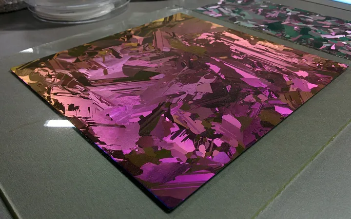
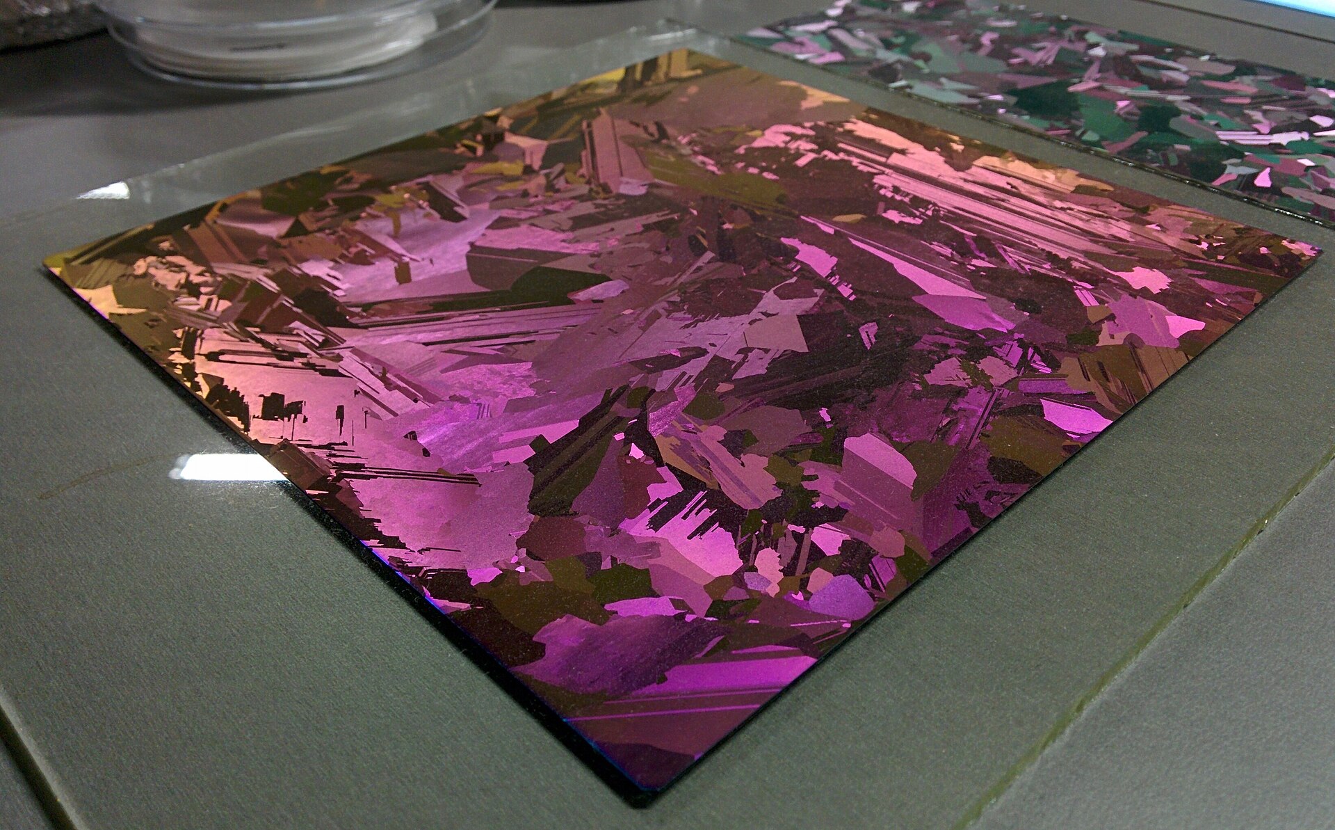
MIT reported a wafer-scale process developed with NY Creates for silicon-photonics chips that are both flexible and transparent. Photonics uses light to carry or process information. The work addresses the physical form of the chip, rather than simply promising a faster processor.
The researchers reported bending tests and optical measurements. Potential applications discussed in the source include devices that follow a curved surface and transparent augmented-reality displays.
Why it matters
Most people encounter computing through a flat screen or a rigid box. This research invites a different question: what becomes possible when an optical component can conform to the object around it?
Our reading is that fabrication is part of interface design. A useful wearable or display needs both the right computation and a physical structure that fits its job.
The next engineering questions
A bendable chip is one component of a complete system. Packaging, connections, power, repair and repeated use still matter. Look for evidence at those system boundaries before translating an attractive materials demonstration into a product expectation.
Understand the idea underneath
Read our illustrated explainer on what light sources, modulators, waveguides and detectors do. It connects this research story to the underlying mechanism, examples and questions to ask next.
Keep the evidence in view.
The report concerns a research fabrication platform. It does not establish availability, price or reliability of a finished consumer product.
Source announcement: . Our source check: . This is an AI-assisted editorial briefing, not an independently reproduced experiment.